Inside a Small Chinese Electronics Factory – From the Archives
นอกจากการดูบทความนี้แล้ว คุณยังสามารถดูข้อมูลที่เป็นประโยชน์อื่นๆ อีกมากมายที่เราให้ไว้ที่นี่: ดูความรู้เพิ่มเติมที่นี่
What is a small Chinese electronics factory like? We’re visiting a factory that does PCB assembly(PCBA), and final assembly (putting the finished product together and putting it in boxes). This is going deep into the Strange Parts archives this is the first ever factory tour video I made, long before I started Strange Parts. I had a much longer beard and no clue what I was doing making videos…
Learn more about Mike’s factory: http://www.szgfydz.com
Thanks to Gordon McCambridge for filming: https://www.instagram.com/gordonmccambridge
See behind the scenes at Strange Parts:
http://twitter.com/strangepartscom
http://instagram.com/strangeparts_com
http://facebook.com/strangepartscom
(some of the following links are affiliate links)
Gear for this video:
Main camera: http://amzn.to/2BfHqiW
Main lens: http://amzn.to/2BAysJQ
Other camera: https://amzn.to/2t1yKWi
Microphone: http://amzn.to/2kNCqHg
Wireless microphones: https://amzn.to/2t12jHJ
Audio Recorder: https://amzn.to/2sXTEWt
Music:
Skating through the City Guustavv (Licensed through http://bit.ly/epidemicsp)
Edited by auram https://www.instagram.com/aurxm/
StrangeParts FactoryTour

Zoom Into a Microchip
The inside of a microchip is a mysterious thing. Here, we zoom into a microchip using a digital SLR camera then we transition to a scanning electron microscope, aka SEM. Although this is an older microchip, many of the same principles still apply to microchip design but with much, much smaller structures measured in nanometers instead of microns.
Learn more:
Education professionals: www.nisenet.org
Public audiences: www.whatisnano.org

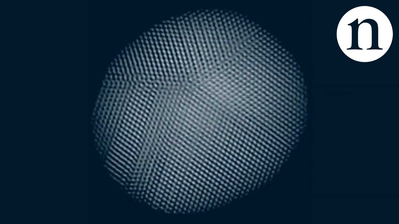
Have you ever seen an atom?
Scientists at the University of California Los Angeles have found a way to create stunningly detailed 3D reconstructing of platinum nanoparticles at an atomic scale. These are being used to study tiny structural irregularities called dislocations.
Read the paper here: http://dx.doi.org/10.1038/nature12009
Sign up for the Nature Briefing: An essential roundup of science news, opinion and analysis, free in your inbox every weekday. https://go.nature.com/371OcVF
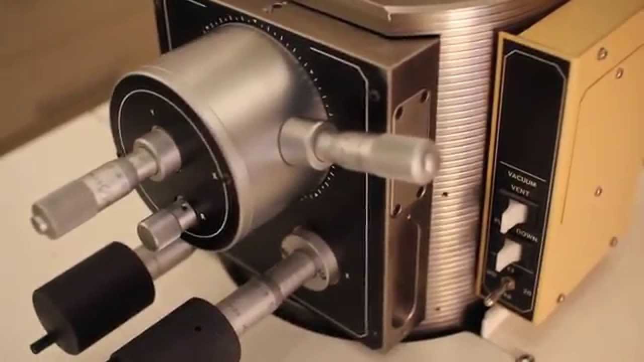
Scanning Electron Microscope (SEM) Demonstration in my living room
This video demonstrates my Scanning Electron Microscope (SEM) that I have at home, in my living room. Please excuse my English, my native language is Swedish, so if anything is unclear please ask me in the comments below, which I will try to reply as often as possible.
More information on: http://www.richardandersson.net/?p=69
The model is a JEOL JSMT200 from the beginning of the 1980s, but even with today’s standards the optics and the performance is quite impressive, with a ca. 10 nm resolution, both a secondary and a backscatter detector and 3D movement/rotation of the sample in 4 axis. However all the controls are manual and you have to capture images using a camera aimed at the screen (traditionally this was done with Polaroid film).
The original manual for the instrument starts with the following description:
The Model T200 Scanning Microscope has been developed under the design philosophy of combining simple operation, simple maintenance, and high performance. Accordingly, quality micrographs comparable to those obtainable by a large instrument can be readily obtained without any special skill. These features together with the various advantages peculiar to the scanning microscope, such as very large depth of focus, wide magnification range, and minimal specimen preparation, make the T200 a most effective instrument for research work, quality control, and as a visual education aid.
Full manual available at: http://www.richardandersson.net/wpcontent/uploads/2015/02/FullManual_small.pdf
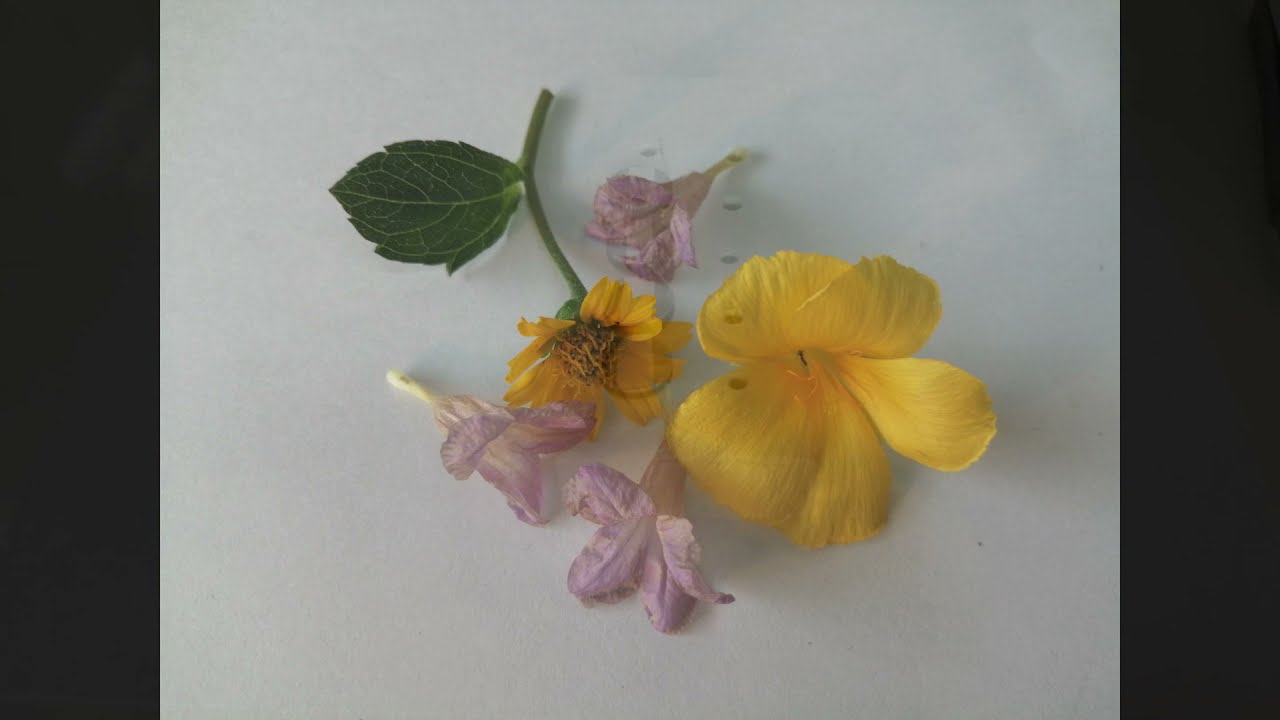
Sample Preparation(2/4)- Pollen, Hair and Butterfly wing-Scanning Electron Microscope –
การติดตัวอย่างละอองเกสร เส้นผม และชิ้นปีกผีเสื้อ บน สตับ เพื่อถ่ายภาพด้วยกล้องจุลทรรศน์อิเล็กตรอนแบบส่องกราด
โดยศูนย์เครื่องมือวิทยาศาสตร์และเทคโนโลยี คณะวิทยาศาสตร์ ม.ศิลปากร
https://www.sustec.com/
นอกจากการดูหัวข้อนี้แล้ว คุณยังสามารถเข้าถึงบทวิจารณ์ดีๆ อื่นๆ อีกมากมายได้ที่นี่: ดูวิธีอื่นๆSales experience